Research Experience
Research Assistant, RPTU, Germany
- Contributed to a robust and efficient design of a low-power pipelined FFT architecture.
- Prepared lecture slides for an academic course.
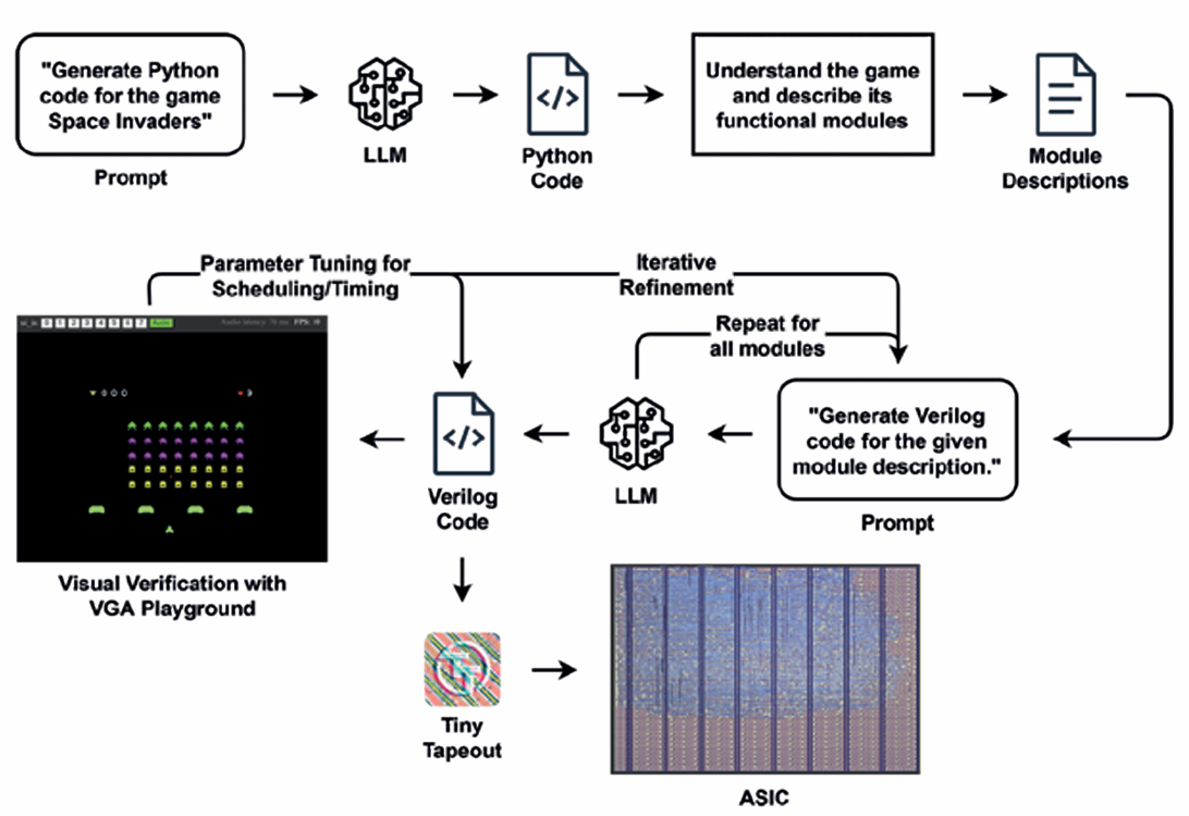
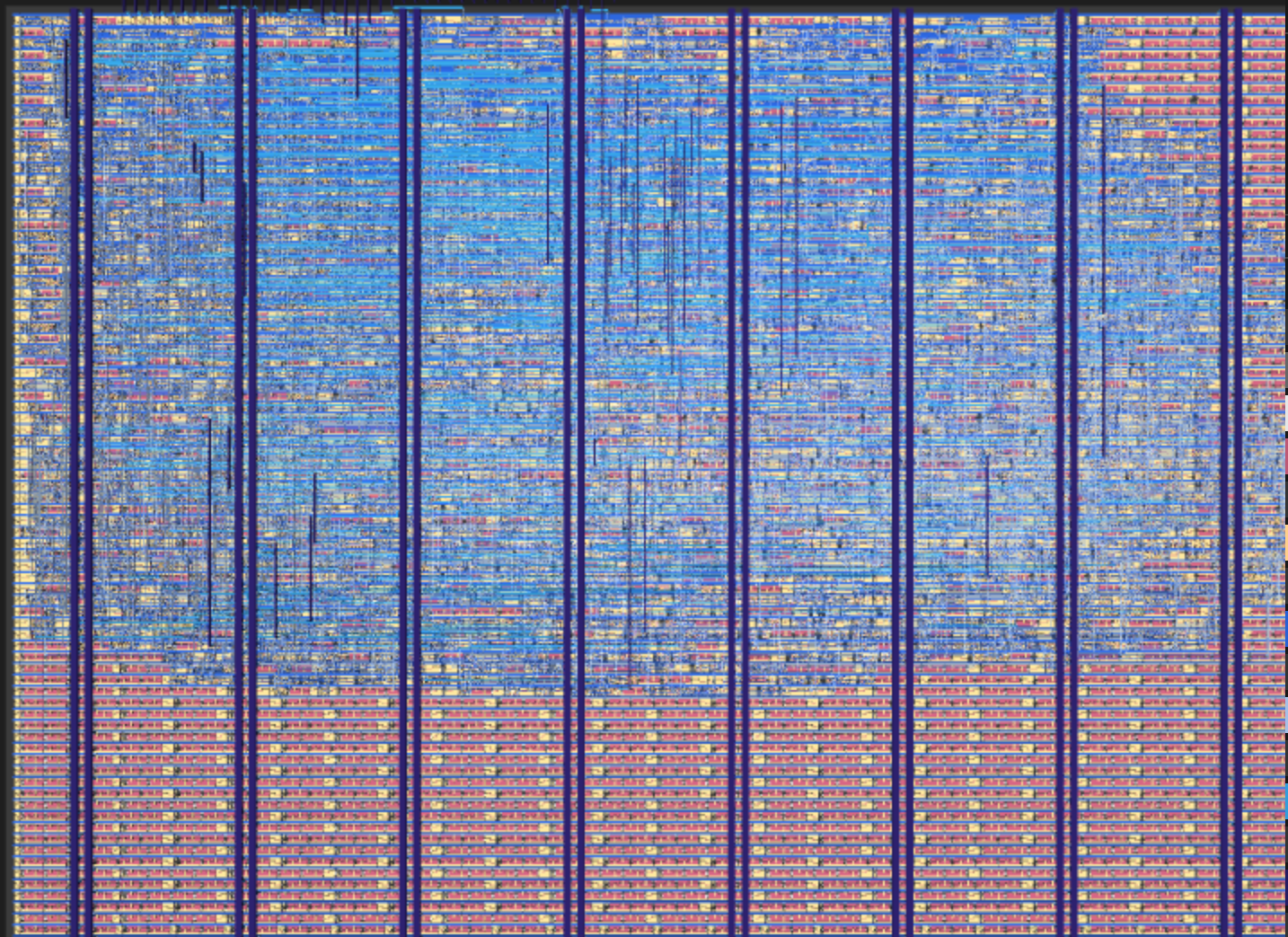
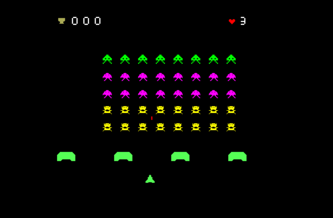
- Led an LLM-guided ASIC design of the Space Invaders Game. The project involved RTL Verilog development, automated RTL-to-GDSII generation, and successful tapeout through TinyTapeout.
MSc Thesis, RPTU, Germany
- Automated a formal methodology for detecting vulnerabilities in non-interfering cryptographic accelerator IPs.
- Applied structural decomposition of RTL designs combined with simulation waveform analysis (Waveform Analysis Language, WAL) to automatically generate formal properties.
- Demonstrated the effectiveness of the method on complex RTL circuits, including cryptographic modules (SHA256, AES, HMAC, and RSA) from the ope-source Caliptra project.
Projects
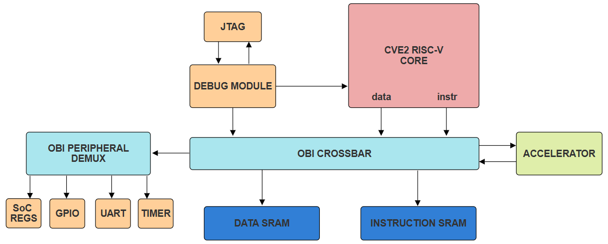
CrocSoC
Full ASIC implementation flow for the CrocSoC design, including functional verification, logic synthesis, floorplanning, placement and routing, and clock tree synthesis using open-source tools.
Affine Transformation Accelerator
An affine transformation is a geometric operation that combines linear transformation functions such as rotation, scaling, shearing, or reflection. These transformations are widely used in areas like computer graphics and image processing. The project implements a 2D affine transformation accelerator that performs these operations directly in hardware using Q8.16 fixed-point arithmetic for efficient computation.
The design was submitted to the Tiny Tapeout open-source platform, where it received recognition and a beautiful Tiny Tapeout cap! I also earned a free tile for a future tapeout as part of the competition.

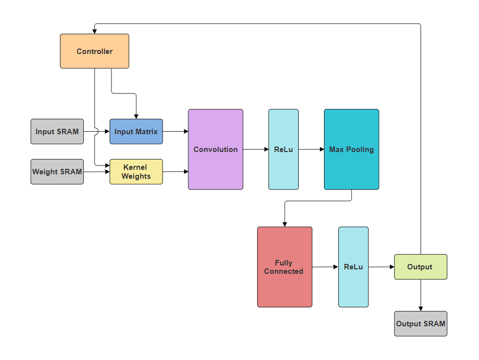
CNN
Designed and implemented a pipelined CNN accelerator supporting a single stage convolution layer, a max pooling layer, and a fully connected layer.
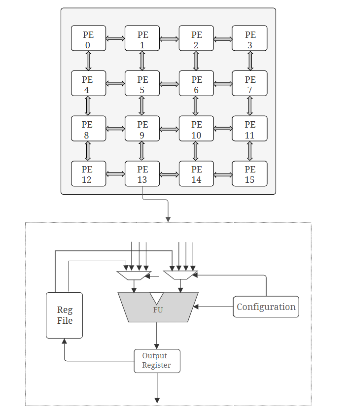
CGRA - Coarse-Grained Reconfigurable Array
This project explores the design of a Coarse-Grained Reconfigurable Array (CGRA) based on an open-source OpenEdgeCGRA project, focusing on efficient processing element architecture and reconfigurable interconnects for accelerated computing.
LLM for Chip design - Space Invaders Game
The Space Invaders project shows how Generative AI can enhance productivity in chip design. We developed a methodology in which prompt descriptions are refined multiple times to generate Verilog code of the game. The design was tapedout using the TinyTapeout platform, resulting in an area of 0.064 mm² and operates at 25 MHz.
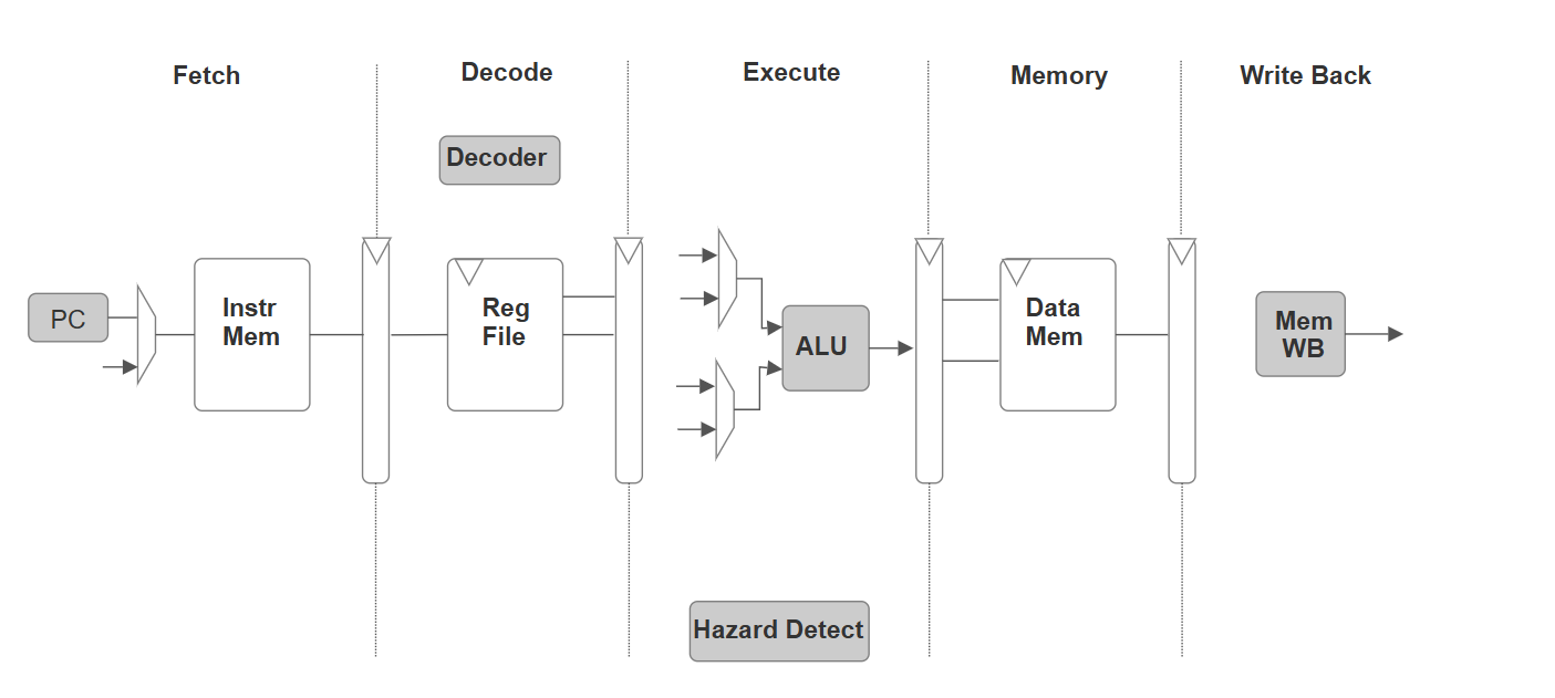
RISC-V Processor (RV32I + Matrix Extension)
This project involves the design and implementation of an RV32I RISC-V instruction set architecture processor, with a focus on optimized pipeline stages and functional correctness. The CPU has pipeline hazard detection and resolution features.
Extended the ISA with custom instructions to accelerate matrix operations.
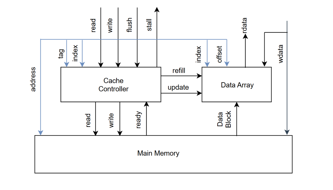
Data Cache Controller
Implemented a direct-mapped, write-through cache and controller in Verilog. It is designed for a single-cycle processor system, this cache efficiently interfaces with an n-cycle latency main memory and optimizes data access.
Specifications & Features:
- The design comprises three main submodules: a) Cache controller with tag array, b) Cache data array, and c) Main memory interface.
- Utilizes a direct-mapped architecture with a write-through, no-write-allocate policy.
- Features a 16-byte (128-bit) cache block size.
- Configurable with 4 cache lines (parameterized for flexibility).
- Supports 32-bit processor data and address buses.
- Integrated with an interleaved memory system, consisting of four 32-bit memory banks.
Learning Resources
Education
- Joint M.Sc. in Embedded Computing Systems, University of Southampton.
- Joint M.Sc. in Embedded Computing Systems, RPTU.
- B.Sc. in Electrical and Electronics Engineering, EIT.